
Z80 CPU architecture
The Z80 CPU is an 8-bit processor which was constructed in the beginning of July 1976, with ideas from Intel 8080. That was before the Intel Company started, and made a better 8080-processor, with backward compatibility and with a lot of new instructions.
The interesting thing about the Z80-CPU is that you can already see the beginning to what was about to become pipelined constructions. The Z80 CPU became soon a very popular processor for small systems - especially later on when the processor was reduced in prize. Now a Z80-processor costs about a dollar, and many are using it out of tradition, which makes it even more popular. If you look at the homepage of Zilog, then you will see that today there is a lot of new variants of chips for Z80 systems, used in a wide range of applications.
The Z80 CPU has a very interesting architecture. First of all it has "fetch/execute overlapping", which means that it's possible to get (fetch) next instruction from memory while the first instruction are executed. This system are also used in the Intel 8080, and other processors from that time. Another thing that are typical from that time is that those processors are CISC-processors, and that they have variable instructions length. The Z80 CPU instructions length can be from one to four bytes long. To increase the Z80 CPU speed most instructions are only one byte long. 252 instructions are one byte, the rest are 2, 3 or 4 bytes long.
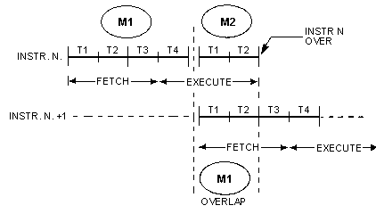
Fig 1. Fetch/execute overlap.
Another aspect in processor- architecture are the number of internal registers, and if they are dedicated to special purposes. The Z80 CPU internal organization is made visible on the figure below:

Fig 2. Z80 CPU internal organization.
It shows on the figure: 20 - 8-bits registers, and 4 - 16-bits registers. The four 16-bits registers are: PC (Program Counter), SP (Stack Pointer) and the two Index-registers, IX and IY.
The 20 - 8-bit registers are grouped into two banks with 10 registers. 8 which can be used together as 4 - 16-bit register-pairs, an 8-bit accumulator and a 8-bit flag-register. The Accumulator A, are used for all calculations. The F-register (flags) are used to determine if the result is positive, negative, zero etc...
The Register-pairs BC and DE are mostly used for counters and storage of part-results. The Register-pair HL can be used in a wide range of instructions mostly as addressing (pointing to memory). The forgotten registers W and Z are only used for internal operations in the processor, like jump to new addresses. (The CPU can only transfer 8 bits at a time, so to transfer (load) a 16-bit address, it will first store it in WZ) .
The registers B, C, D, E, F, H, L, W and Z can be changed very fast with B', C', D', E', F', H', L', W' and Z', with the instruction EXX. For this purpose a MUX is used, which is the fastest way to change the value in 9 registers with 9 others. The A and F are switched with A' and F' with the instruction EX AF,AF'. This finesse are mostly used with interrupt routines, so that the main program are using the main set of registers and the interrupt routine are using the EXX registers, this speeds up the interrupt routine, which can be important in embedded applications.
The Z80 CPU has with Intel, inspired to the global processor development and are still alive today more than 20 years after it's construction and it seems like it will continue to live many years more.
Info source: Programming the Z80 by Rodney Zaks. From SYBEX (ISBN: 0-89588-094-6)
Figures:
This page was original made by Gunnar in Swedish.
And then translated to English by me
I have also translated and shaped the graphic figures.